Fast inorganic characterization of polymer defects is crucial for quality control and is complementary to molecular spectroscopic techniques such as FT-IR and Raman spectroscopy. The latest advances in integrating XRF technology enable bulk analysis together with small spot analysis and elemental mapping on a single platform. The ED core, using SumXcore technology, is capable of simultaneous analysis of the elemental composition of small spots. This enables much faster elemental mapping than commonly used WD-XRF mapping options.
This data sheet describes the small spot mapping, SSM, of a dark spot or defect in a polyolefinic sample.
Fast inorganic characterization of polymer defects is crucial for quality control and is complementary to molecular spectroscopic techniques such as FT-IR and Raman spectroscopy. The latest advances in integrating XRF technology enable bulk analysis together with small spot analysis and elemental mapping on
a single platform. The SumXcore technology of the Zetium spectrometer incorporates an ED core capable of simultaneous analysis of the elemental composition of small spots. This enables much faster elemental mapping than commonly used WDXRF mapping options. Measurement times can be optimized further with the dedicated small spot fluorescence collection optics of SumXcore’s HiPer SSM option. This application note describes the small spot mapping (SSM) of a dark spot or defect in a polyolefinic sample.
The Polymers edition of the Zetium X-ray spectrometer is a fully integrated XRF spectrometer, complete with an X-Y sample handler and state-of-the-art software and application templates for a successful calibration setup for polymers and plastics. To enable SSM capability, the spectrometer was equipped with an ED core, high-precision turret translation mechanics for sample positioning and a high-resolution camera for sample imaging.
The sample was a solid disc of 40 mm in diameter and 2 mm in thickness. As XRF needs almost no sample preparation, the sample was put directly in the small spot mapping sample holder, clamped and measured.
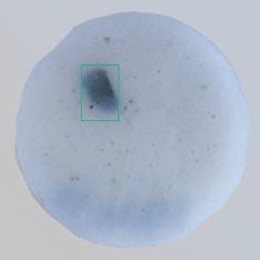
After placement of the polyolefinic sample in the SSM loading position (Figure 1), an image was taken using the high-resolution camera. From this image (Figure 2) an area of interest was chosen. In this case, the darker-colored defect was mapped using 40 spots in a 4 mm by 7 mm area. (Figure 3). The spot size was 500 µm with a step size of 1000 µm (100 µm minimum possible).

Figure 1. Ployolefinic sample with defect
Figure 2. Sample view for small spot mapping area selection
Figure 3. Sample view with projected small analysis area positions
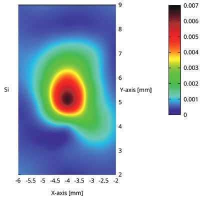
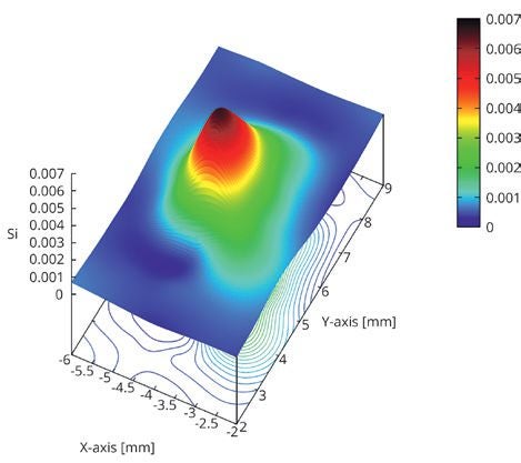
Full elemental analysis for the selected area was achieved in 76 minutes using the standard SumXcore configuration for small spots. With the HiPer SSM option, such a map can be obtained in just 16 minutes at 4 kW or 21 minutes at 2.4 kW. Inspection of the element maps revealed that silicon was unevenly distributed between the darker-colored area and the more uniform-colored bulk of the material. Figure 4 displays the relative concentrations of silicon over the mapped area and Figure 5 is a 3D contour plot of the same area. In both figures, blue represents a low intensity and red/black represents higher intensities

Figure 4: Distribution map of silicon for the selected area

Figure 5. 3D contour plot of silicon for the selected area
Higher concentrations of silicon in the colored area of the sample can indicate inhomogeneous filler distribution. The lack of higher concentrations of aluminum, titanium, phosphorus and calcium also suggests that catalyst residues and additive distribution are not causing this darker color. Being able to demonstrate the silicon agglomeration in the sample suggests improvements in filler dispersion which can contribute to the reduction of defects and improved product homogeneity. SSM using the ED core functionality, often combined with molecular spectroscopic techniques like FT-IR and Raman, is therefore vitally important for origin defect investigations in polymers. Moreover, by selecting fewer spots, defects can be investigated for full elemental composition in even under 5 minutes.
Fast small spot elemental mapping of defects in polymeric samples is easily achieved using the capabilities of the ED core. The simultaneous analysis of many elements reduces the measurement time significantly. The high-precision turret translation mechanics for sample positioning and a high-resolution camera for sample imaging enables a thorough investigation of small defects. Complementary to FT-IR or other molecular spectroscopic techniques, fast small spot elemental mapping completes the picture in the search for clues of defect origins in polymers and plastics.