High resolution X-ray diffraction
Analysis of layered structures

Analysis of layered structures

High-resolution X-ray diffraction (HRXRD) is a collection of application techniques for the non-destructive analysis of mostly layered, nearly-perfect crystalline structured materials. The structural parameters that can be revealed and quantified are essential for the successful application of such materials.
Most of today’s modern semiconductor device structures are epitaxially grown from the gas phase onto a substrate made from silicon, silicon-germanium, III-V and II-VI compounds. These films are nearly-perfect crystalline films containing a relatively low dislocation density.
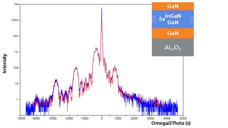
Film properties are largely determined by their compositional and structural parameters. Information such as layer thickness, composition, strain, relaxation and structural quality is obtained by measuring rocking curves and reciprocal space maps using high-resolution X-ray optics. The spatial distribution of defects can be visualized by X-ray diffraction imaging methods such as X-ray topography.
High-resolution X-ray diffraction experiments on epitaxial layers, heterostructures and superlattice systems require an highly monochromatic X-ray beam with a well defined wavelength spread and a low angular divergence.
Malvern Panalytical’s X'Pert³ MRD (XL) and Empyrean systems fulfill the requirements of HRXRD. A wide selection of hybrid monochromators and high-resolution monochromators are available to meet the specific resolution requirements of different materials. The unique PreFIX mounting allows quick and simple setup changes without the need for realignment.
Epitaxy and Smoothfit software enables operators as well as advanced users to analyze rocking curves, reciprocal space maps and wafer maps. Rocking curves can be simulated and fitted using patented algorithms.