Overview
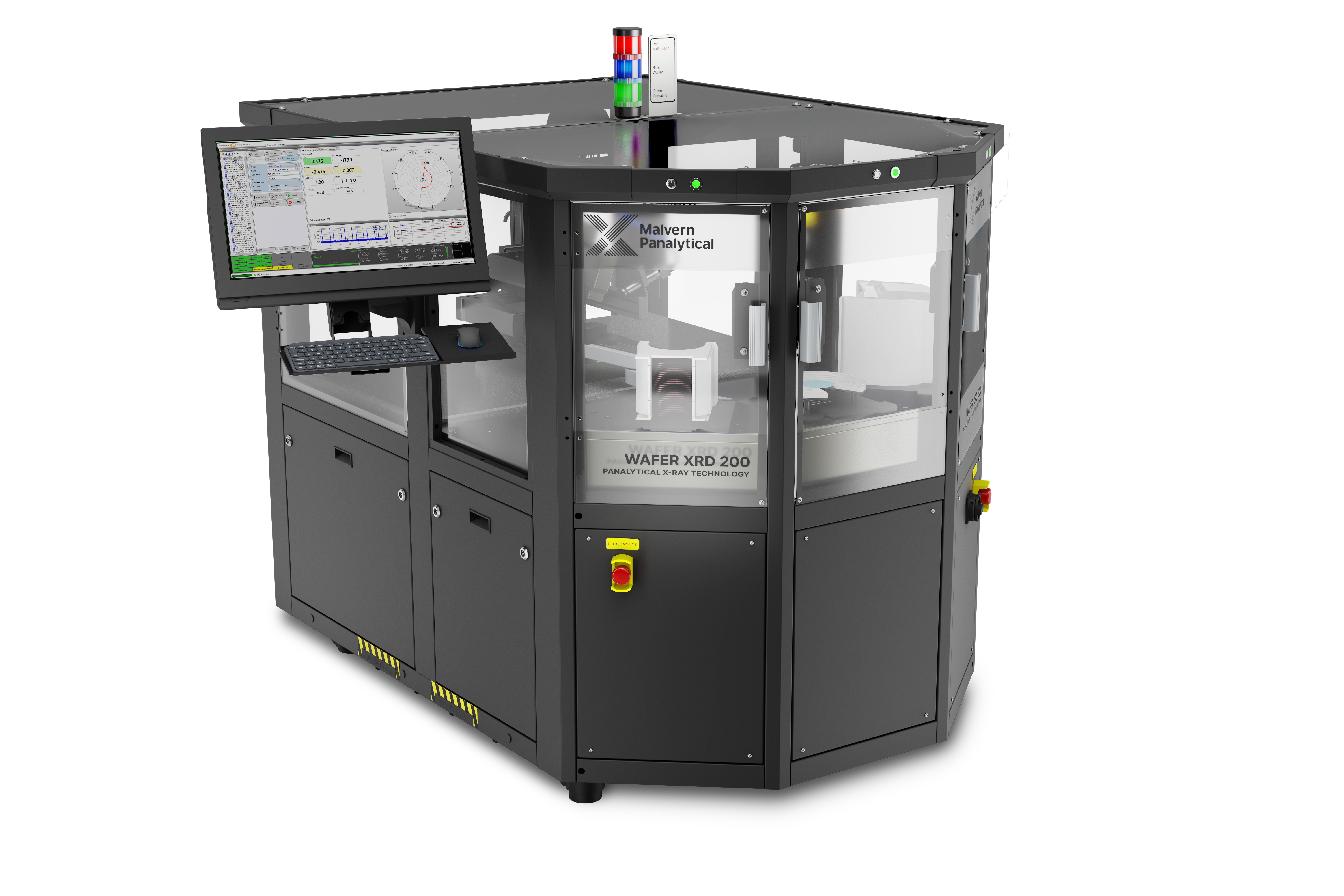
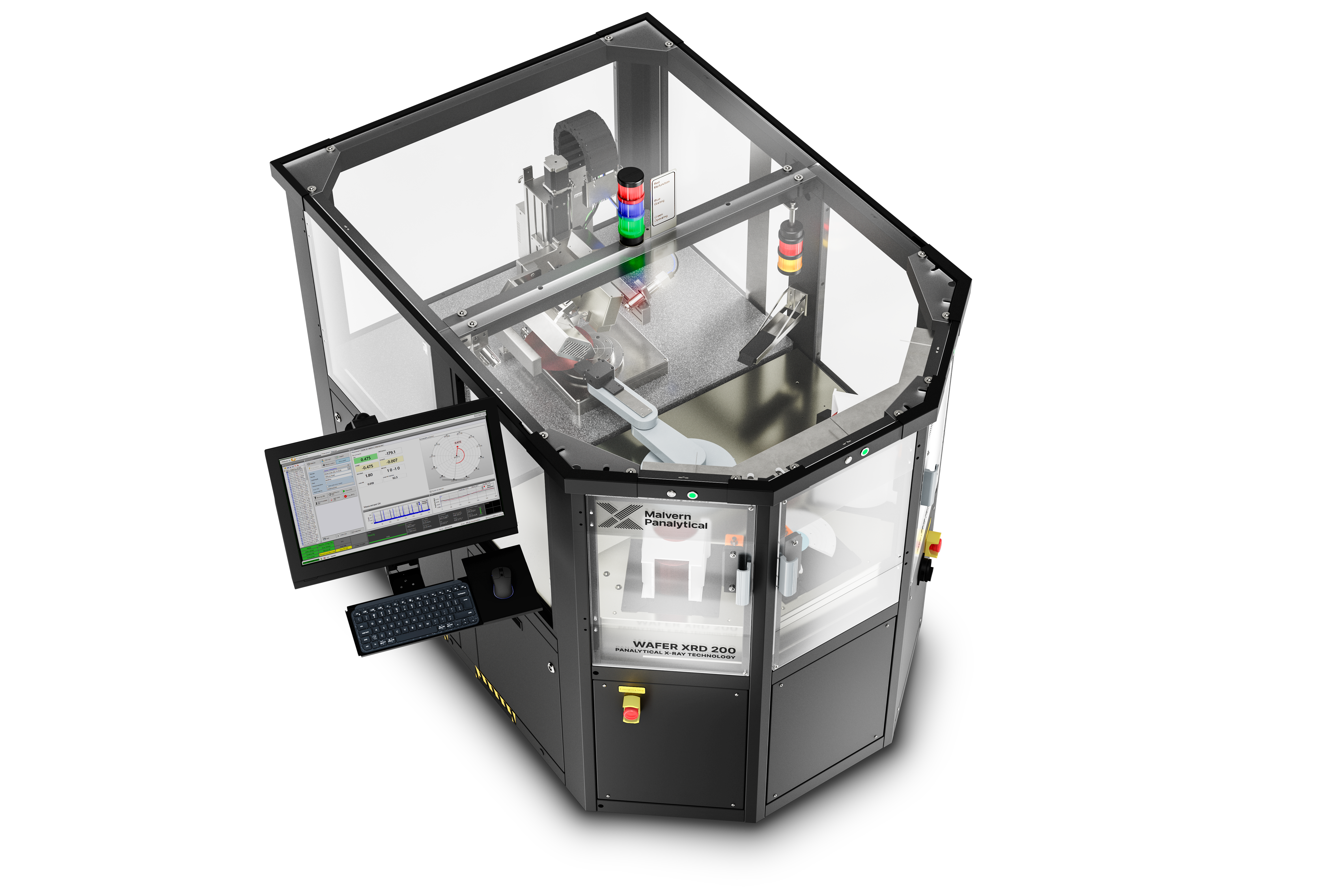
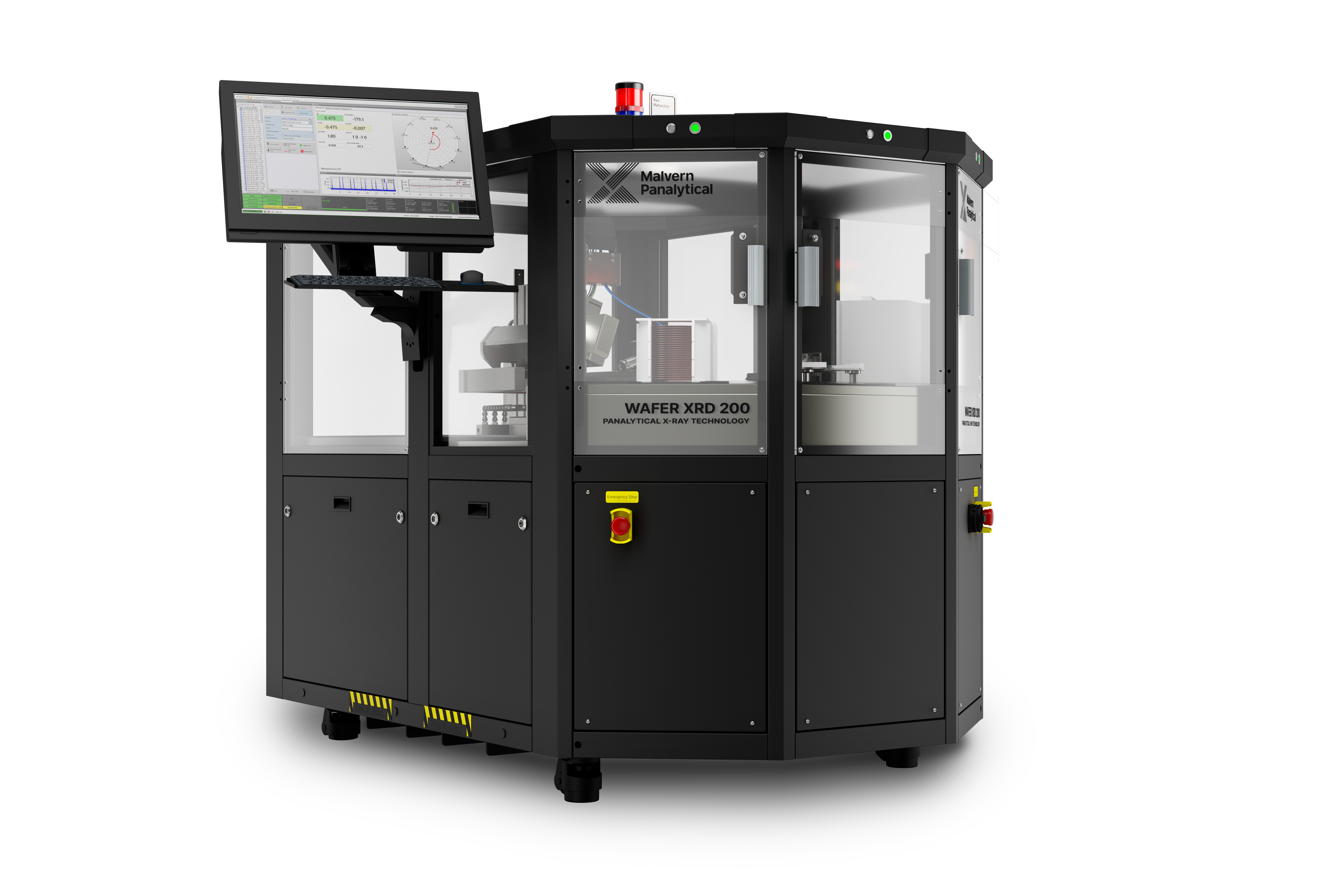
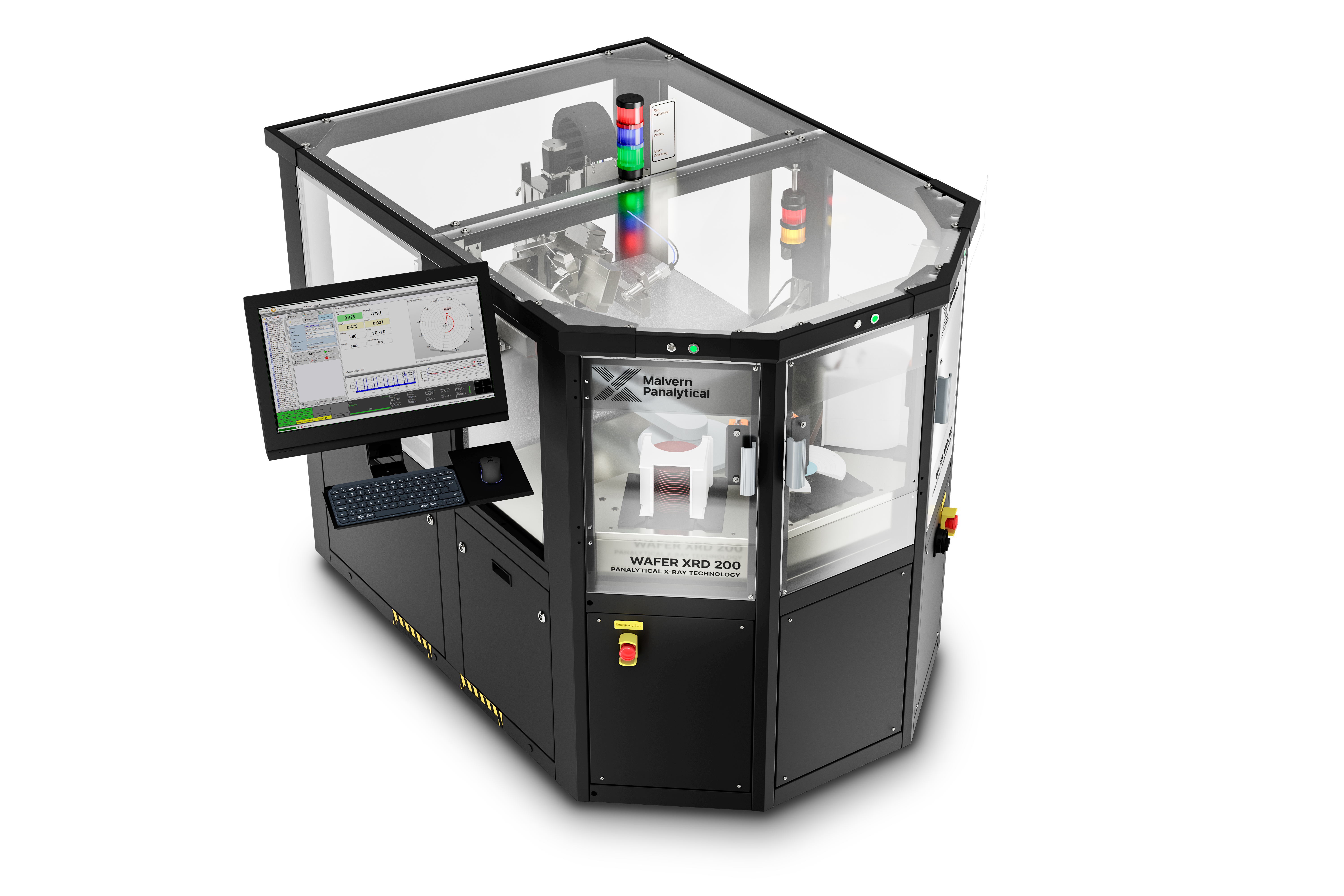
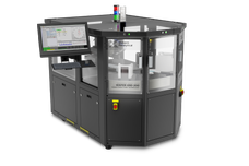
Wafer XRD 200 is your fully equipped and automized X-ray diffraction system for wafer production and research, providing high speed and accuracy.
Designed to fit seamlessly into your process line, it delivers key data such as crystal orientation, geometric features recognition like notches and flats, distance measurements and further options such as resistivity much more.
Features and Benefits
Ultra-fast and precise: Azimuthal scan method
The azimuthal scan method requires only one measuring rotation to gather all the necessary data to fully determine the orientation, which delivers the results within 10 seconds while not compromising accuracy.
The sample is rotated 360o, with the X-ray source and detector positioned to achieve a certain number of reflections per turn. These reflections enable the orientation of the crystal lattice to be measured in relation to the rotation axis with high precision of up to 0,003o.
Fully automated handling and sorting
Able to measure a full cassette of 25 wafers in less than 10 minutes, Wafer XRD 200 does this completely independently, making it a powerful and efficient element in your QC process.
Operating costs are low for the Wafer XRD 200, thanks to its low energy consumption and air-cooled X-ray tube – no water cooling is required.

Easy connectivity
The instrument can be easily integrated into existing processes in production environments using its various MES, SECS/GEM and similar interfaces.

Deeper insights
Wafer XRD 200 makes you understand your materials like never before, being able to measure:
- Crystal Orientation
- Notch position, depth, and opening angle
- Flat position and length
- Diameter
- Resistivity etc.
Versatile and Flexible
Wafer XRD 200 is well-equipped for production environments in which a large number of samples need to be analyzed quickly.
It can measure samples with up to 200mm of diameter, with high stability due to measuring one defined material from the below:
- SiC
- GaAs
- Si
- Al2O3 (sapphire)
- InP
- Any other single crystalline materials
Key Applications
-
- Production and processing
- Automation is a necessity in this fast-paced industry – and the Wafer XRD 200 is leading the charge as a practical, powerful solution to manage wafer handling, sorting, and in-depth measurements of crystal orientation, optical notch and flat determination, resistivity measurements, and other important parameters. Experience the increased productivity for yourself!
- Quality control
- Understanding your materials accurately and quickly is the key to great quality control, and the Wafer XRD 200 is the ideal solution. Using the ultra-fast Omega-Scan method, it determines crystal orientation within a single measurement – giving you your results in five seconds. With additional functionality including resistivity measurement and geometric feature determination the Wafer XRD 200 offers unparalleled efficiency and versatility for production quality control.
- Materials research
- Not every busy environment is a production environment – Wafer XRD 200 is equally equipped to provide high-throughput analysis in R&D environments alike. Able to characterize hundreds of different materials, from Si, SiC, and GaAs to quartz, LiNbO3, and BBO, the Wafer XRD 200 has the versatility to support your materials research and innovation assisting you in shaping the future of semiconductor technology.
Specifications
| Throughput | 10000+ Wafer per Month |
| Wafer geometry | On request |
| Tilt precision | 0.003 |
| XRD axis vs notch / flat position | 0.03° |
Support
Support services
- Phone and remote support
- Preventive maintenance and checkups
- Flexible Customer Care Agreements
- Performance certificates
- Hardware and software upgrades
- Local and global support
Expertise
- Turnkey solutions for elemental and structural semiconductor metrology
- Automation and consultancy
- Training and education

