Surface characterization


Surface characterization is the comprehensive analysis of a material's surface, focusing on its structure, composition, and physical attributes. This involves various techniques to measure surface properties such as roughness, morphology, chemical composition, and more.
The goal is to obtain detailed insights into the surface layer, which plays a crucial role in determining the material's overall performance and interaction with its environment.
Surface characterization encompasses a range of methods and techniques designed to analyze the properties of a material's surface. Each method offers unique insights, allowing researchers to understand various aspects such as morphology, composition, and physical properties.
Different surface characterization methods provide complementary information. For instance, microscopy techniques can reveal surface morphology and structure at high resolutions, while spectroscopy techniques offer detailed compositional analysis. Other specialized methods measure properties like surface energy, roughness, and film thickness. Together, these techniques enable a comprehensive understanding of surface characteristics, which is crucial for material development, quality control, and performance optimization.
Malvern Panalytical is a leading provider of analytical instruments that offer precise and comprehensive surface characterization.
With a focus on innovation and accuracy, Malvern Panalytical's instruments are used in various industries to enhance material performance and quality.
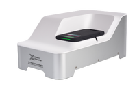
Automated imaging for advanced particle characterization
The Morphologi range includes instruments that provide precise particle characterization through automated static image analysis.
These instruments are ideal for measuring particle size, shape, and distribution, which are critical parameters in surface characterization.
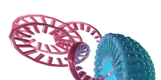
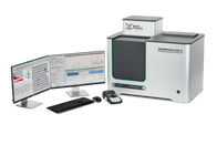
Light Scattering for every application
The Zetasizer range features instruments that utilize dynamic light scattering (DLS) and electrophoretic light scattering (ELS) to measure particle size, zeta potential, and molecular weight. Particle size is a fundamental physical parameter that may govern or influence a material's property, reactivity, transport and general efficacy. Whilst particle size in itself is not a surface property this information coupled with other data, such as surface area, will give insights into the material under study.
One surface property that may be key to your material's performance is surface charge or Zeta potential. Zeta potential is a measure of a particle, in dispersion, apparent charge – this property can be key to dispersion stability or its end-use performance.
Surface characterization techniques play a crucial role in various industries and fields of research. By providing detailed insights into the properties of material surfaces, these techniques enable the development and optimization of materials for specific applications.
Below are some of key areas where surface characterization is essential.
In materials science, surface characterization techniques are fundamental for understanding and improving material properties. Researchers use these techniques to study the surface morphology, composition, and physical attributes of materials, leading to the development of new materials with enhanced performance and functionality.
Techniques such as scanning electron microscopy (SEM) and atomic force microscopy (AFM) are used to analyze surface treatments and coatings, ensuring they meet the desired specifications for applications like corrosion resistance and wear protection.
X-ray photoelectron spectroscopy (XPS) and Raman spectroscopy help in identifying the chemical composition and molecular structure of materials, facilitating the development of advanced materials with tailored properties.
Nanotechnology involves the manipulation of materials at the nanoscale, where surface properties become increasingly significant. Surface characterization techniques are vital for analyzing nanostructures and ensuring their proper function and stability.
Techniques such as transmission electron microscopy (TEM) and AFM provide detailed images and profiles of nanostructures, allowing researchers to study their morphology and interactions at the atomic level.
XPS and Auger electron spectroscopy (AES) are used to investigate the chemical states and elemental composition of nanomaterials, which are critical for applications in catalysis, drug delivery, and sensor technologies.
The semiconductor industry relies heavily on precise surface characterization to ensure the quality and performance of semiconductor devices. Surface characterization techniques help in detecting impurities, measuring thin film thickness, and analyzing surface topography.
Techniques such as SEM and surface profilometry are used to inspect the surface morphology and roughness of semiconductor wafers, identifying defects that could affect device performance.
Ellipsometry and XPS are employed to measure the thickness and composition of thin films used in semiconductor devices, ensuring they meet the stringent requirements for electronic applications.
Surface characterization is essential for the development and application of coatings and thin films, which are used to enhance the surface properties of materials.
Contact angle measurement and surface profilometry are used to evaluate the wettability, adhesion, and roughness of coatings, ensuring they provide the desired protective or functional properties.
Ellipsometry and Raman spectroscopy are used to analyze the thickness, optical properties, and molecular structure of thin films, which are crucial for applications in optics, electronics, and photovoltaics.
Automated imaging for advanced particle characterization
Light Scattering for every application